
Project descriptions
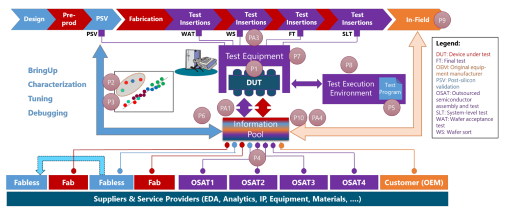
The following projects are currently being conducted within the Graduate School. The following diagram visualizes the positioning of the individual projects within today's semiconductor test processes.
Click on a project's title to learn more about the project and the involved investigators.
Projects of the 2nd Funding Phase
Supervisors:
Prof. Dr.-Ing. Dr. h. c. Michael Weyrich
Institut für Automatisierungstechnik und Softwaresysteme
Pfaffenwaldring 47
D-70569 Stuttgart
Jun.-Prof. Dr.-Ing. Andrey Morozov
Institut für Automatisierungstechnik und Softwaresysteme
Pfaffenwaldring 47
D-70569 Stuttgart
Co-supervisor: Khaled Karoonlatifi, Matthias Werner, Advantest
Researcher: Thorben Schey
Abstract
This project is devoted to Digital-Twin based methods for earlier development of optimized post-silicon tests for chips with mixed-signal circuits. Post-manufacturing testing, like wafer testing and final testing of chips, ensures that each chip delivered contains no manufacturing defects that harm its functionality. Although mixed-signal circuits make up only a relatively small number of the circuits integrated into a chip, the development of tests for chips that also feature mixed-signal circuits takes a disproportionately long time. Today, the development of corresponding tests starts only after the production of the first chips. According to our vision, implementing the post-manufacturing or so-called post-silicon tests should be started before producing the first chips. This will accelerate time-to-market and enables parts of the Test Program development before the first physical devices are available. For this objective, we will use the Digital Twin of a chip, i.e., an extensive software system that leverages models and data of an original chip to represent, predict, and simulate its behavior for test generation purposes. This willrequire the adaptation and extension of the so- called Virtual Test infrastructure, which is today in use for pre-silicon validation needs, for the earlier post-manufacturing test development requirements. Furthermore, such a Digital Twin environment will optimize post-silicon test scheduling. Today, mixed-signal post-silicon tests are usually performed sequentially using automated test equipment, so-called testers. By modeling post-silicon test constraints, an optimal parallel schedule can be obtained.
Supervisors:
Prof. Dr. Ilia Polian
Institut für Technische Informatik
Abt. Hardwareorientierte Informatik
Pfaffenwaldring 47
D-70569 Stuttgart
Prof. Dr. Jens Anders
Institut für Intelligente Sensorik und Theoretische Elektrotechnik
Pfaffenwaldring 47
D-70569 Stuttgart
Co-supervisor: Frank Mielke, Advantest Siamak Salimy, Hprobe)
Researcher: Karthik Pandaram
Abstract
In this project, we will consider digital combinational CMOS logic and investigate the responses of defective structures under static and dynamic magnetic fields in three domains: logical (changes in the digital Boolean function); timing (impact on the observable delay); and current (quiescent and transient IDD). In addition, we will explore our methods for emerging devices.
Supervisors:
Co-supervisor: Jose Moreira, Advantest
Researcher: Viet-Dung Nguyen
Abstract
Transceiver front-ends for millimeter-wave wireless communications, such as driven by 5G and 6G systems, are increasingly integrated together with antenna arrays within compact module form factors. The production test and calibration of such modules requires new over-the-air (OTA) measurement concepts. This project shall investigate new OTA concepts, addressing electromagnetic and antenna aspects as well as strategies and requirements for test and calibration of large arrays.
Supervisors:
Prof. Dr. Jens Anders
Institut für Intelligente Sensorik und Theoretische Elektrotechnik
Pfaffenwaldring 47
D-70569 Stuttgart
Co-supervisor: Sarah Rottacker, Klaus-Peter Behrens, Advantest
Researcher: Tim Strobel
Abstract
This project explores the challenges that silicon lifecycle management introduces into the chip design process and, more importantly, the opportunities that it brings to the area of test. In particular, we will focus on the possibilities associated with digital on-chip sensors combined with edge AI in the tester to collect and process the data very efficiently at run-time. Further, we will also investigate the possibility of on-chip online learning on the collected data.
Supervisor:
Co-supervisor: Martin Zimmermann, Advantest
Researcher: Tarek Ashraf
Abstract
The research will be focused on the advanced technology nodes of transistors at the 5nm, 3nm and 2nm in which new 3D structures are employed as well as new gate materials like hafnium zirconium are used. We will focus on several reliability problems such transistor self-heating and transistor aging. We will also focus on developing novel test methods for the purpose of improving IC yield in latest advanced technology node.
Supervisor:
Co-supervisor: Frank Mielke, Advantest, Siamak Salimy, Hprobe
Researcher: Munazza Sayed
Abstract
We will focus on studying the interactions between semiconductor device physics and external magnetic fields. The studies will be carried out for both transistors and memory cells. Emerging technology nodes and in particular the ferroelectric memories will be in detail investigated.
Supervisor:
Prof. Dr.-Ing. Bin Yang
Institute of Signal Processing
and System Theory
Pfaffenwaldring 47
D-70569 Stuttgart
Co-supervisor: Yiwen Liao, Advantest
Researcher: Yang Yang
Abstract
Feature selection in machine learning (ML) in general or variable selection in semiconductor test deal with the problem of selecting a subset from a large number of input features or variables. In this proposal, we use the term variable selection because the input quantities under consideration, i.e. the stimuli, operational conditions and tuning knobs during PSV, are mostly measured physical variables (e.g. voltage, current, power, frequency, time) and not features calculated from raw data.
Variable selection can be supervised or unsupervised. In this project, variable selection is supervised because we aim to select input variables to best predict one or a few target variables. The current approach in PSV, which is addressed in our previous project, is to select 3 to 5 relevant input variables from up to a few hundreds. The test engineers plot one target variable as a function of the selected input variables and use this visualization in debugging the DUT (which variables cause the DUT to fail?) or tuning (which variables influence the performance of the DUT most?).
Supervisor:
Prof. Dr. Dirk Pflüger
Institut für Parallele und
Verteilte Systeme
Universitätstraße 38
D-70569 Stuttgart
Co-supervisor: Sarah Rottacker, Advantest
Researcher: Linus Bantel
Abstract
Performance tuning of semiconductors plays an important role in testing since it is decisive for the yield in production and time-to-market. As produced chips necessarily deviate from their specs, for example due to highly complex designs and tight process integration, tuning has to ensure that their observed performance stays within their specifications under all allowed (environmental) conditions. Robustperformance tuning poses a complicated optimization setting with peculiar challenges. In a previous project, we have developed a novel approach, where an efficient and flexbile tuning law is learned with reinforcement learning that is robust against faulty devices in the training data.
The current setting is that of Post-Silicon Validation, where learning is based on test data for a first batch of produced chips. This project will extend the current static setting to dynamic scenarios. The aim is intelligent tuning that continuously adapts to shifts in the data, for example due to process variation and changing conditions in high-volume production. This raises challenging questions, for example of how to adapt machine learning models without full re-training, and how to deal with non-standard data. You will approach these questions for example with methods from active learning, reinforcement learning, and higher-dimensional approximation.
Supervisors:
Prof. Dr.
Steffen Becker
Institut für Softwaretechnologie
Abt. Zuverlässige Softwaresysteme
Universitätsstraße 38
D-70569 Stuttgart
Prof. Dr.
Stefan Wagner
Institut für Softwaretechnologie
Abt. Software Engineering
Universitätsstraße 38
D-70569 Stuttgart
Co-supervisor: Gerd Bleher, Martin Heinrich, Jochen Palmer, Advantest
Researcher: Siddiqui Sidra
Abstract
High-quality test software is critical for high-quality hardware testing. Complex software plays a vital role in large-scale hardware testing. Test programs allow hardware testers to deal with the complexity of modern chips and enable them to automate the tests. Yet, the software itself also becomes large and complex leading to hard to understand failures. In this project, you will develop methods and tools to support software testers in understanding failures that are uncovered during software testing. For this, you will explain these failures by the context and possible influencing factors, the executed code and possible code fixes. The method and tool development will iteratively validated using empirical studies.
Supervisors:
Co-supervisor: Georg Karich, Yiwen Liao, Advantest
Researcher: Marc Rivinius
Abstract
Over the past two decades the semiconductor industry has shifted from an integrated device manufacturer (IDM) dominated market towards the fabless model with its multitude of highly specialized service providers such as foundries, fabless designers, test houses, and electronic design automation (EDA) software providers. During the production process, large amounts of data are generated and have to be analyzed and monitored, e.g. data from fabrication equipment, measurements from the testing process, or supplementary data from managing the production process itself.
In order to analyze this data, techniques based on machine learning (ML) are increasingly employed. Applications for ML in the semiconductor production include among others to predict the later behavior of devices based on early data and to improve the classification of devices during tests (i.e. binning). However, a large amount of the currently generated data is sensitive and the data owners are unwilling to share this data without security and privacy guarantees, since it contains insights into business-critical information such as yield, characteristics of devices, and operational parameters. This information needs to be protected from unwanted disclosure or industrial espionage. Besides intellectual property issues, the data may also involve customer data which cannot be forwarded to ML service providers legally.
The goal of this project is therefore to enable parties in the semiconductor production chain to carry out ML computations on large data sets in a federated but privacy-preserving way, i.e., in a way where parties do not need to reveal their data or models to other parties. For this purpose, cryptographic techniques, in particular, multi-party computation (MPC), are used, adapted, and further developed.
Associated Projects
Not funded by Advantest
PhD Student:
Supervisor:
Preliminary title:
M. Sc. Zahra Paria Najafi Haghi
Prof. Dr. rer. nat. habil.
Hans-Joachim Wunderlich
"Variation-aware Test Method to Increase the Reliability of Nano-scale Devices"
1. Main goal: As the technology shrinks, SoCs suffer more from reliability vulnerabilities such as early life failures. Current test methods using conventional fault models like "stuck at fault" or "transient fault", even with high fault coverage, still result in high rate of Early Life Failure (ELF) which shows that conventional fault models are not sufficient anymore. Circuit timing as an indicator for reliability can be used to consider another group of defects which are called marginal defects. Marginal defects may produce small amount of extra delay to the paths of a circuit but it's not big enough to be detected in the conventional manufacturing test. Due to their special characteristics which is indicating some marginal hardware and imperfections, they degrade further when they go in the field and make the device fail after a short period of time.
On the other hand, all modern devices suffer from some process variations. Tests without considering the impact of process variation are no longer valid. That's why variation-aware test came into action. Process variation results into some deviation from the nominal delay of a circuit. This delay can be small enough to pass the manufacturing test which is not a thread to the reliability, since they will stay the same during the life time of the circuit and make no failure. The problem here is that, the duration of the delays due to process variation can be in the same order of magnitude with the delays due to marginal defects. This makes the detection of marginal defects even more challenging. Furthermore over detecting of the slow cells due to process variation will decrease the yield, whereas they can be appropriately speed binned and used as lower performance part.
In this work, we aim to present a novel variation-aware test method which is able to distinguish faulty circuits with marginal defects from fault-free circuits which are just slow due to process variation.
2. Description: The whole process will come in 3 main steps: 1-Modeling, 2-Characterizing, 3-Classification
In order to classify the faulty and fault-free devices (in our case faulty means devices with marginal defects and fault-free means slow circuits due to process variation), first these classes should be modeled to be able to investigate their behavior under different controllable or settable conditions. Therefore standard cells will be defined to model cell with process variation as the fault free class and with additional marginal defect injected to them to model the faulty class.
Next step after modeling the fault-free and faulty classes, is to investigate their behavior under different conditions which gives the characterizing of these two classes. Some controllable points which may have different impact on these two classes need to be investigated. There are many controllable points that can be considered such as "supply voltage" or "temperature". Circuit timing and in particular "propagation delay" is an important observation vector which is used to investigate and compare the behavior of these two classes. Time simulation is being used first at transistor level for standard cells and then at higher abstraction levels to simulate the behavior of the circuit. The time simulation and then the fault simulation with injected marginal faults will provide the characteristics of the cells which are the "functions" of the controllable point. As an example different supply voltages are being applied to these two classes, and two classes of propagation delays which are functions of supply voltage will be collected.
Next and final step is classiffication. These two "classes of functions" will be used as training data to the machine learning algorithms. These machine learning algorithms then are able to classify new cells by using their functions of the controllable points such as supply voltage function, to determine which class they belong to.
With having the characteristics of the cells and being able to classify them, final goal which is the classification of a complete circuits can be achieved. Cell characteristics can be used to make faulty models, BIST or offline testing of a complete circuits. Direct mapping from defined fault-free and faulty cells to the cells used in the circuit under test (CUT) and in addition, interconnects between cells will be investigated to apply the test for a complete CUT.
As a result of all discussed before in this part, a novel and intelligent variation-aware test will be introduced which is able to detect realistic marginal defects in presence of process variation. This will reduce the early life failure of a circuit and as a result increase the reliability while keeping the yield high.
This doctoral project is funded by the German Research Foundation (DFG) under grant WU 245/19-1 (FAST).
PhD Student:
Supervisor:
Preliminary title:
Prof. Dr. rer. nat. habil.
Hans-Joachim Wunderlich
"Dependable Integration of Reconfigurable Scan Networks for Test and Diagnosis"
An extensive number of instruments is needed to facilitate cost-efficient bring-up, debug, test, diagnosis, and adaptivity in the field. Reconfigurable Scan Networks (RSNs)[1, 2] provide a exible way to access such instruments. At the same time, the dependability properties of the device-under-test (DUT) can be effected through an improper RSN integration. In this doctoral project, the problem of dependable RSN integration and its use during runtime operation are investigated. The functional safety and fault-tolerance, as well as security compliance of the RSN with the properties of the functional design, are addressed.
The main goal is to investigate the dependability properties of RSNs and to provide an automated framework, capable to generate a dependable RSN for a given DUT. Various dependability aspects of RSNs and corresponding methods and algorithms for the RSN analysis and consequent integration are investigated. The doctoral project aims to achieve the following goals:
- Security-compliant RSN: An RSN can be potentially misused to sniff or spoof the data if additional data channels between instruments are introduced through the RSN integration. Only those dependencies between instruments, which are present in the DUT, should exist in the RSN. An accurate security compliance analysis of an RSN must be developed to guide the construction of a secure RSN. Both methods to repair an existing RSN and to automatically generate a dependable RSN, for a given DUT must be investigated.
- RSN for offline and online test: Reconfigurable Scan Networks have been initially proposed for offline test and diagnosis of integrated circuits. However, RSNs can also be efficiently reused for online test and diagnosis. Optimizing criteria for RSN generation as access latency, throughput or area overhead, must be formalized and the corresponding RSN architectures have to be developed.
- Functionally safe & fault-tolerant RSN: A single fault in a scan design can lead to inaccessibility of a safety-critical instrument and consequently might lead to a system failure. An integrated RSN must be fault-tolerant to provide reliable test and diagnosis results for DUT even in presence of faults during online and offline system operation. Moreover, the RSN itself has to remain testable and diagnosable.
- Dependable RSN: Pareto-optimal solution, considering the aforementioned dependability aspects and hardware costs, must be proposed.
To ensure the security compliance of a given RSN with the DUT we developed an approach to accurately calculate the data paths between the instruments introduced through the RSN integration and analyzed, whether those data paths are a subset of initial paths in the DUT. If any new paths are introduced, the RSN has to be modified in a most cost-efficient way [3].
To ensure efficient operation of an RSN for offline test and diagnosis, such criteria as hardware overhead or power con- sumption can be considered. Safety-critical components must be tested periodically and concurrently to the main functionality of the design. They must be accessed in runtime through an RSN having a low access latency. For periodic access to such instruments as BIST, a heuristic must set up an optimal schedule, considering the retargeting capabilities of RSNs. RSNs are also used to perform access to the aging monitors. Since the number of monitors can be large, access to them must be optimized to approach all of them in a reasonable amount of time.
To guarantee the reliable operation of DUT such fault-tolerance techniques as selective hardening, DMR/TMR or ECC can be applied, and reliability instruments, such as aging monitors or Built-In Self-Test (BIST), can be integrated on chip. Error detection and error correction codes can be used to detect erroneous output values of the original design and mask them to a limited extent. An RSN structure, capable to transport error indicators efficiently and autonomously, will be developed. The dependable RSN must be at least as fault-tolerant as the original DUT and certain aforementioned methods with acceptable hardware overhead, e.g. selective hardening, can be applied to an RSN. If a fault occurs in an RSN itself, the fault location must be detected and possibly corrected within a short time. Robust hierarchical RSN can be augmented with additional error propagation paths, providing short fault detection and reaction period.
This doctoral project is funded by the German Research Foundation (DFG) under grant WU 245/17-2 (ACCESS).
References
- "IEEE Standard for Test Access Port and Boundary-Scan Architecture," IEEE Std 1149.1-2013 (Revision of IEEE Std 1149.1-2001), pp. 1-444, May 2013.
- "IEEE Standard for Access and Control of Instrumentation Embedded within a Semiconductor Device," IEEE Std 1687-2014, pp. 1-283, Dec. 2014.
- N. Lylina, A. Atteya, P. Raiola, M. Sauer, B. Becker, and H.-J. Wunderlich, "Security Compliance Analysis of Reconfigurable Scan Networks," in Proceedings of the IEEE International Test Conference (ITC'19), 2019.
PhD Student:
Supervisor:
Preliminary title:
Prof. Dr. rer. nat. habil.
Hans-Joachim Wunderlich
"Online Evaluation of system health state"
Main goal:
The system health state indicates whether a system will be able to meet the performance specifications now and for some future time. It goes beyond just monitoring its current state and testing for correctness. But also, it predicts how long it will continue to function correctly. This type of predictive evaluation is motivated by the increasing reliability requirements and widespread use of semiconductor systems. The current state of the art employs sensors and monitors to gather, interpret, analyze, and utilize data streams in order to evaluate the system health state at runtime. Power consumption, current, temperature, and timing behavior of a circuit are among the health indicators of the circuit. This information is, however, collected with an additional hardware overhead and with a performance penalty due to additional workload. Additionally, every additional hardware component is another lifetime challenge since they will all age, as well.
In this doctoral project, one of the main objectives is to reduce the additional overhead and costs of the instrumentation and extract as much information as possible from the usual system behavior. Built-in-self-test (BIST) is a popular technique which allows hardware to test itself and evaluate the responses. A BIST architecture consists of a pattern generator that produces required patterns; a large volume of test responses is then compressed into signatures through different strategies. We utilize the BIST architecture in this study to assess the system health state at a lower hardware and performance cost. We use adaptive voltage and frequency scaling mechanisms to keep track of how the circuit behavior changes over time and investigate the effect of each degradation on the signatures of a BIST architecture. We use this investigation to train Machine Learning (ML) models to predict the health state.
Challenges:
The main research challenges comprise Analysis and Classification. As we explore defect mechanisms, our aim is to investigate how reliability threats behave under variant conditions. We can characterize these different reliability threats by studying their behavior under various frequencies and voltages.
Machine Learning techniques will be used to classify observed changes over time and to estimate the remaining lifetime.
The following scientific challenges need to be addressed in this doctoral study in order to assess a system's health
- Analyzing the hardware, and looking in defects that how they may involve overtime
- Analyzing the circuit behavior and see how it changes overtime based on the defect
- Measurement of the aging process using the data from the early life stages
- Classification of defects according to their behavior
- Runtime prediction of the system health state using Machine Learning methods

PhD Student:
Supervisor:
Preliminary title:
Prof. Dr. rer. nat. habil. Ilia Polian
"AI-Driven Device-specific Tester Calibration"
Abstract:
Artificial Intelligence driven Device Tester Calibration (AI-DeTeC) aims to improve the quality of the semiconductor product (yield) and the efficiency of the semiconductor test process. By correlating data from the Device Under Test and the test cell (Automated Test Equipment - ATE, loadboard, pogo, socket) using Artificial Intelligence based methodologies, AI-DeTeC aims to prognose the optimal ATE Calibration interval and provide actionable insights on yield detractors.
On a conceptual level, AI-based methodologies for analysis of data from various sources during test will be established, with the purpose to improve both: the quality of the product (yield) and the efficiency of the test process itself (overall equipment effectiveness / OEE). Goal is to develop a high-level predictive AI model to bring together test-related data from the DUT (both its regular responses and acquisition of on-chip parameters); the loadboard measurements; the tester-internal equipment data; the history of maintenance events; and yield-related information, as shown in the figure below. This model should be able to predict ATE-related variables such as calibration intervals and relevant yield detractors.
Projects of the 1st Funding Phase
Supervisors:
Prof. Dr. Jens Anders
Institut für Intelligente Sensorik und
Theoretische Elektrotechnik
Pfaffenwaldring 47
D-70569 Stuttgart
Prof. Dr. Ilia Polian
Institut für Technische Informatik
Abt. Hardwareorientierte Informatik
Pfaffenwaldring 47
D-70569 Stuttgart
Co-supervisor: Dr. Matthias Sauer, Advantest
Researcher: Nourhan Elhamawy
Test quality, defined as the absence of test escapes (defective circuits that had passed post-manufacturing test), is the ultimate target of testing. Customers apply system-level test (SLT) to circuits that already have been tested post-fabrication and reportedly identify test escapes. The objective of this project is to understand the nature of such hard-to-detect failures. Establishing a better understanding of SLT and making it more effective and efficient could drastically improve the economy of circuit design and manufacturing.
A number of theories exist for the type of failures that cause SLT-unique fails that are missed by post-manufacturing tests:
- Complex defect mechanisms with subtle parametric or intermittent manifestations that are not adequately covered by standard fault models. The test coverage of such defects can be improved by the use of more advanced defect-oriented models.
- Systematic ATPG coverage holes: Insufficient coverage of structures such as clock domain boundaries, asynchronous or analog interfaces, clock distribution networks and other sources of unknown values. Standard automatic test pattern generation (ATPG) tools tend to classify faults in such structures as “untestable” even though they can manifest themselves during normal operation of the device.
- Marginal defects exposed only during system-level interactions: Subtle defects, in particular related to timing, in “uncore logic” of complex multicore systems on chip (SoCs), i.e., logic that is part of the SoC but does not belong to a core.
The specific objectives of the project are as follows:
- To establish a theoretical and systematic understanding of SLT-unique fails, identifying specific mechanisms leading to such fails and their manifestation conditions (e.g., hot-spots).
- To create an experimentation environment where SLT-unique fails can be reproduced and practically investigated.
- To explore solutions that prevent or address SLT-unique fails. These can include guidelines for “clean” circuit designs that do not give rise to coverage holes (e.g., use of well-defined asynchronous protocols for clock domain crossings); design for testability (DFT) methods that address specific weaknesses known to the designer or DFT engineer; extended ATPG methods that can detect defects missed by regular ATPG, or methods to create effective and efficient SLTs that specifically target SLT-unique failure mechanisms.

The project is structured into three tasks according to the three above-mentioned scientific objectives. The more theoretical Tasks 1 and 3 deal with SLT-unique fails and solutions to counteract them, respectively. Task 2 will establish a complete evaluation and experimentation flow that can be used for practical demonstration of SLT-unique fails and studies of applicable solutions. Figure 1 summarizes the planned project structure and the interaction of its theoretical (red) and practical (blue) parts. An SLT evaluation platform ① will be created and SLT-unique fail conditions ② from Task 1 will be incorporated into this platform. Based on the outcome of experiments ③, solutions for the SLT-unique fails ④ from Task 3 (e.g., addition of special DFT logic) will be incorporated into the SLT evaluation platform ①, thus closing the loop.
Supervisors:
Prof. Dr.
Thomas Ertl
Institut für Visualisierung und Interaktive Systeme (VIS)
Abteilung
Graphisch-Interaktive Systeme
Universitätsstraße 38
D-70569 Stuttgart
Prof. Dr.
Daniel Weiskopf
Visualisierungsinstitut (VISUS) und
Institut für Visualisierung und
Interaktive Systeme (VIS)
Allmandring 19
D-70569 Stuttgart
Dr.
Steffen Koch
Institut für Visualisierung und Interaktive Systeme (VIS)
Abteilung
Grafisch-Interaktive Systeme
Universitätsstraße 38
D-70569 Stuttgart
Researcher: Andrés Lalama
Visual analytics (VA) is a subfield of visualization research that aims at tightly incorporating automatic methods and interactive visualization techniques into coherent approaches.
This project aims to tackle challenges occurring in post-silicon validation with visual analytics methods. We will use VA in helping with the visual analysis of a number of sub-problems in validation of first post-silicon systems, in order to speed up problem analyses and make them more reliable and accountable. In addition, we propose to develop an interactive workflow that integrates the sub-analysis tasks to increase the efficiency of chip validation.
The project will include the following tasks:
- Assist the user by identifying and visualizing methods in order to display large amounts of complex high-dimensional data sets effectively.
- Ease the navigation when browsing through high-dimensional space. Provide visually supported sub-tasks, which can be suitably integrated into a coherent interactive analysis workflow.
- Development of suitable interaction techniques for selecting and determining subspaces based on the overview visualization. That will assist the user with processing statistical significance.
- Mitigate the interpretation of correlations as causal relationships by keeping them apart.
Its goal is to develop new visual analytics approaches in close cooperation with chip testing experts, and to organize successful visual solutions into coherent interactive analysis workflows. We pursue a client-server architecture with a web-based frontend that assist with both debug and tuning scenarios.
Through all of the tasks a user-oriented process that encompasses meetings, workshops, and evaluation sessions to tests (parts) of interactive visual approaches together with domain experts at different project stages.
Supervisor:
Prof. Dr. Dirk Pflüger
Institut für Parallele und
Verteilte Systeme
Universitätstraße 38
D-70569 Stuttgart
Co-supervisor: Jochen Rivoir, Advantest
Researcher: Peter Domanski
InPost-Silicon Validation (PSV), devices under test (DUTs) are examined to identify tuning parameters such that the DUTs meet their specifications under all operating conditions. This project aims to determine a tuning law or sweet spots for tuning based on randomly generated test data from one or multiple DUTs. The goal is to develop a generic, data-driven approach that automatizes the PSV tuning task, copes with less assumptions, and scales well. We have to deal with up to a few hundred input parameters (conditions and tuning parameters) and several output parameters. Depending on the context, one refers to parameters, variables, or dimensions.
Conventionally, the identification of tuning configurations relies on classical point-wise optimization methods. Point-wise optimization methods such as Powell’s method assume certain properties of the objective function or approximate the objective to fulfill these properties. Given the properties, the methods implement different iterative strategies to converge to the optimal tuning configuration. This approach is insufficient and makes it difficult to allow more flexibility and robustness with respect to function properties. An approach based on random search is also impractical due to the high-dimensional parameter space and the related curse of dimensionality. However, flexibility and robustness are essential in PSV because the properties of the objective function are unknown even for experts. Due to process variations in the manufacturing process, devices are black-box functions with varying performances. In case of severe problems in manufacturing, devices can even be faulty. Moreover, classical point-wise methods are not well suited to optimize mixed data types in high-dimensional parameter spaces and thus often perform poorly in such setups.
As DUTs have very unique properties including heterogeneous parameters (numerical, integer, nominal) and non-smooth dependencies, the aim is to learn a tuning law in an adaptive, self-learning way. Therefore, we aim to follow the path of learn-to-optimize and examine approaches based on reinforcement learning for deep neural networks, active learning, and novel approaches to optimization.
The resulting methodology will lead to a deployable tuning law that is robust and flexible. The project is closely related to the projects P6 “Deep learning based variable selection for post-silicon validation” and P2 “Visual Analytics for Post-Silicon Validation”. P2 will use the results and the gathered knowledge about the input-output relationships to visualize and possibly guide tuning as well as test case generation in interaction with human experts. P6 will benefit from robust solutions that detect or compensate influences of faulty devices to employ deep learning variable selection methods based on test data, while our project can benefit from information about learned sets of input variables.
Supervisors:
Co-supervisor: Dr. Matthias Sauer, Advantest
Researcher: Sebastian Hasler
Abstract
Semiconductor testing plays an important role in the semiconductor manufacturing process. The tests not only ensure the quality of individual chips, but the data obtained during the tests is used to improve the manufacturing process itself. Often manufacturers use third-party services to perform the tests and evaluate the test data, as this requires specialized expertise. Since the test data and the models and methods to evaluate the data, such as machine learning models, are typically highly sensitive trade secrets, on the one hand, manufacturers are reluctant to share their test data with third-party evaluation services, and on the other hand, the services do not want to reveal their evaluation models and methods.
The idea of the project is to use, further develop, and adapt secure cryptographic protocols, to protect the digital assets in a globalized and distributed semiconductor manufacturing flow.
Supervisors:
Prof. Dr.
Steffen Becker
Institut für Softwaretechnologie
Abt. Zuverlässige Softwaresysteme
Universitätsstraße 38
D-70569 Stuttgart
Prof. Dr.
Ilia Polian
Institut für Technische Informatik
Abt. Hardware-
orientierte Informatik
Pfaffenwaldring 47
D-70569 Stuttgart
Prof. Dr.
Stefan Wagner
Institut für Softwaretechnologie
Abt. Software Engineering
Universitätsstraße 38
D-70569 Stuttgart
Co-supervisor: Dr. Matthias Sauer, Advantest
Researcher: Denis Schwachhofer
Description of the problem tackled
Modern Systems-on-Chip (SoCs) are extremely powerful but also highly complex products. They incorporate heterogeneous components, such as multiple processor cores, on-chip memories, application-specific digital circuitry or input-output interfaces. System-Level Test (SLT), where actual application software is run on the circuit, has emerged as an important additional test method for such SoCs. SLT can be run by the circuit manufacturer in the final stage of production; or by the buyer of the circuit (e.g., an automotive Tier-1 supplier who will integrate the circuit into a product) as part of incoming quality control. SLT can also be used during the post-silicon characterization phase where a circuit’s extra-functional properties are measured on a population of several hundreds or thousands of “first-silicon” circuits. To facilitate test and characterization, many SoCs include an infrastructure of sensors and monitors that collect data about the actual values of parameters and make it available to the test program and to the automatic test equipment. We refer to this infrastructure as Design-For-X or DFX, where “X” stands for “testability”, “resilience”, “yield”, “diagnosis” and other related terms. DFX infrastructure is also used to provide self-awareness to an SoC when it is deployed in the field after it has passed the test.
The proposed project focuses on generation of SLT programs with desired characteristics. Its main goal is to provide automated methods to produce SLT programs with extra-functional properties, like power consumption, based on model-driven performance stress test generation from high-level software architecture models. It will also make first steps towards coverage metrics for SLT, leveraging latest results from the field of integration test. The project will incorporate self-awareness of the SoC under test achieved through on-chip sensors organized in a DFX infrastructure and coordinated and assisted by the ATE during test application. For example, an SLT program may aim at achieving a certain power consumption and to this end apply stress tests while monitoring a current sensor, stopping once the desired value has been reached

The project focuses on three methodical challenges:
Parametric property management: capture and control the parametric, or extra-functional (timing and power), behavior of an SoC and its components at software level. We plan to provide compact models of software-level artifacts (C-level instructions or basic blocks) and consider the SLT program as a composition of such software-level artifacts associated with parametric properties.
Coverage metrics for SLT test: SLT program generation on SoC level bears similarity to black-box integration testing of complex systems such as automobiles. Such systems consist of a large number of components that are highly complex on their own and can impossibly be modeled in full detail. We will conduct first evaluations of “graybox” models with partial information, and of coverage concepts recently introduced and applied in the context of black-box integration testing.
Harnessing and supporting device’s self-awareness: To achieve a good control of extra-functional properties, we will leverage self-awareness features which many today’s SoCs provide, namely on-chip sensors and monitors located in different SoC components (red circles in the figure) accessible through the SoC’s DFX infrastructure.
Supervisor:
Prof. Dr.-Ing. Bin Yang
Institute of Signal Processing
and System Theory
Pfaffenwaldring 47
D-70569 Stuttgart
Co-supervisors: Jochen Rivoir and Raphael Latty, Advantest
Researcher: Yiwen Liao
Post-silicon validation deals with the test of devices under test (DUT) in order to find and correct design bugs before mass production. For doing this, up to several hundreds of input variables or features are recorded. They characterize the input stimuli to the DUT, various tuning parameters and environmental conditions. At the same time, some target variables are calculated from the responses of the DUT. By studying the relationship between the input and target variables, design bugs and unexpected effects have to be detected, localized and mitigated. Today this is still done manually by experienced engineers. However, several hundreds of input variables are too much for visualization and manual inspection. Since a single target variable is typically related to a few input variables, the selection of relevant input variables for a specific target variable becomes a crucial problem.
Numerous traditional methods have been developed for the task of feature or variable selection, e.g. wrapper/filter/embedded methods. They were successful in some applications and failed in others. The goal of this project is to take a fresh look at the old problem of variable selection from a new perspective of deep learning. Deep learning in this context does not mean a deep and large neural network as a black box for everything. We rather mean an increasing number of recent and successful ideas and architectures developed for deep learning. Some of them have a strong relationship to the problem of variable selection. We aim to adopt these ideas to variable selection and to develop new approaches which hopefully outperform the traditional methods. Of course, also a combination of the traditional methods and new approaches is highly desirable.
Two first ideas of deep learning based variable selection to be studied are:
- Attention-based variable selection. An attention network is used to compute an attention vector containing weights to select or deselect the individual input variables. Here, the selection is considered as a binary classification problem (select or deselect) and the corresponding weights denote the probabilities of selection. The weighted input vector is the input for a second evaluation network which evaluates the ability of the weighted input vector to predict the desired target variable.
- Concrete autoencoder (AE). AE is a well-known architecture to learn a nonlinear hidden lower-dimensional representation for the given input. This technique is a nonlinear extension of the conventional principal component analysis (PCA). The bridge between AE and variable selection is the use of a Concrete distribution, a continuous relaxation of discrete random variables. By doing this, the continuous-valued weight matrix of the encoder can be trained by normal backpropagation. During inference, each column of the weight matrix approaches a one-hot vector for a zero temperature limit and thus selects a single feature.
This project is closely related to two other projects: P2 “Visual analytics for post-silicon validation” and P3 “Self-learning test case generation for post-silicon validation”. P2 uses the results from this project to visualize the relationship between the target variable and the selected input variables. P3 employs self-learning methods to generate more test cases which will improve the variable selection. On the other hand, the results of variable selection will provide an improved understanding of the input-target-relationship to guide the self-learning test case generation.
Supervisor:
Prof. Dr.-Ing. Ingmar Kallfass
Institute of Robust Power
Semiconductor Systems
Pfaffenwaldring 47
D-70569 Stuttgart
Co-supervisor: Dr. Christian Volmer, Advantest
Researcher: Athanasios Gatzastras
This project addresses the research area “Advanced design methodologies for testing next generation and beyond RF devices” by proposing a miniaturized and multi-functional frequency extension into the high millimeter-wave frequency range for RF testing. One goal of this project is to cover the frequency range from 20 to 86 GHz to enable testing for applications such as 24 GHz ISM i.e. from K-band to E-band, including important frequency ranges like 77-79 GHz for automotive radar or 81-86 GHz fixed wireless point-to-point links by using high-speed semiconductor technologies (see Figure 1).
 Figure 1: Frequency range of the INWAVE project
The transceiver module is designed to be coupled to a 20 GHz RF base card from Advantest. The project covers the most challenging components of an entire transceiver chain including RF up-conversion, RF multi-pole switching, RF adaptive power amplification, RF filtering and LO multiplication over the entire frequency range (see Figure 2).
 Figure 2: Signal processing and transceiver chain
In order to meet the challenging requirements of wide frequency range, high linearity and high output power and at the same time achieve a high level of system integration, it will probably become necessary to design and combine different parts of the system in different semiconductor technologies, e.g., RF-CMOS, GaN, InP or GaAs.
Therefore, this project is divided into two main phases. In the first project phase a deep investigation of all commercially available technologies will be made. After that a line-up will be created to allow a detailed simulation of each sub-block. Two approaches will be considered: a hybrid version that will select the most suitable semiconductor technology for each element of the design, and a compact system-on-chip (SoC) version based on a state-of-the-art CMOS process (e.g., 22nm FD-SOI). After this first phase a decision about the target technology will be made together with Advantest to initiate the second phase of this project.
At the beginning of this phase the circuit design and layout with a full-3D simulation of the whole system will be performed. In order to optimize the design, three fabrication cycles are planned. Depending on the chosen packaging technology the assembly will also be designed. Finally the project ends with the testing and measurement of the developed system.
Supervisors:
Prof. Dr.
Steffen Becker
Institute of Software Technology
Reliable Software
Systems
Universitätsstraße 38
D-70569 Stuttgart
Dr.-Ing.
André van Hoorn
Institute of Software Technology
Reliable Software
Systems
Research Group
Universitätsstraße 38
D-70569 Stuttgart
Prof. Dr.
Stefan Wagner
Institute of Software Technology
Software Engineering
Universitätsstraße 38
D-70569 Stuttgart
Co-supervisor: Martin Heinrich, Advantest
Researcher: Maik Betka
Software plays a vital role in large-scale hardware testing. Test programs allow hardware testers to deal with the complexity of modern chips and enable them to automate the tests. A tester operating system and development environment (TOSDE) connects the customer test programs to the test system with the device under test (DUT). The TOSDE is a complex high data-volume software, for which it is extremely challenging to provide and assure the requested level of correctness, robustness, and performance. This is due to the ecosystem being many-fold and only partially under the control of the automatic test equipment (ATE) platform developers. For instance, typical test system hardware handles millions of instructions per second (MIPS) running an embedded software that communicates with the tester operating system. Customers define and/or generate test programs. As a result of growing chip complexity (Moore's law), the test program complexity and the resulting data volumes are growing exponentially. Hence, this leads to performance-related questions about the TOSDE, including data transfer rates to local discs and network drives. The customer devices and the respective test programs are not available to the TOSDE team for intellectual property reasons. It is vital that the software-intensive TOSDE is of high quality to support the effectiveness and efficiency of the hardware testers. In particular, it needs to be correct, robust to a wide variety of uses by hardware test programs, and perform efficiently to minimize test time.
The objective of the project is to develop and evaluate a novel approach to analyze and optimize software test suites for correctness, robustness, and performance. The particular focus is the support for testing high and exponentially growing data-volume software in a context in which unknown code (test programs) will run on top of this software, which has not been considered by previous approaches. Generating tests using fuzzing seems like a promising approach to tackle the vast space of possible test programs. Yet, to overcome the problems discussed above, we need to find a novel combination of tailored techniques from functional (e.g., coverage analysis, fuzzing, mutation testing) and non-functional testing (e.g., operational profile based scalability testing), as well as model-based performance analysis (e.g., anti-pattern detection, what-if-analysis) to be able to decide what is interesting and important to test so that we get enough performance to handle the high data-volume while reducing the test execution time to feasible levels.
The project will be structured into the following research areas:
- Area 1 (Test Suite Analysis) will investigate and propose methods to analyze the effectiveness of test suites in the context of complex, high data-volume software such as TOSDEs.
- Area 2 (Test Suite Optimisation) will investigate and propose methods to optimize test suites regarding the trade-off between effectiveness and test execution time.
- Area 3 (Test Case Generation) will utilize the effectiveness analysis results from area 1 to automatically generate test cases to achieve desired levels of the identified effectiveness metrics.
- Area 4 (Combination of Manual and Generated Test Cases) will provide the methods to support the adequate combination of manually created and automatically generated test cases. The goal is to provide methods to optimize the interplay by analyzing and optimizing these hybrid test suites, building on the methods from areas 1-3.
- Area 5 (Validation and Evaluation) comprises all activities conducted to assess the developed methods. The experimental evaluation will be conducted by using publicly available open-source systems as well as by applying them to an industry-leading TOSDE software.
Supervisor:
Jun.-Prof. Dr. Hussam Amrouch
Institute of Computer Architecture and Computer Engineering
Semiconductor Test and Reliability (STAR)
Pfaffenwaldring 47
D-70569 Stuttgart
Co-supervisor: Dr. Martin Zimmermann, Advantest
Researcher: Florian Klemme
Problem Description and Project Focus
Existing state-of-the-art FinFET technology has enabled the semiconductor industry to continue transistor scaling below 22nm. Unlike other promising technologies such as Fully Depleted Silicon-On-Insulator (FD-SOI), which is unable to provide scaling beyond 12nm, the massive production of commercial chips at the 7nm technology node using FinFET technology has already started in 2019 and offered by the major semiconductor vendors like TSMC and Samsung. However, at such transistor feature sizes, FinFET technology reaches limits in scaling and replacing it with another technology becomes inevitable to further continue scaling. Among many innovations, nanosheet transistors are gaining an ever-increasing attraction and they have been already adopted by some semiconductor vendors such as TSMC for the next generations.
The research project aims at investigating the new kinds of challenges, that such new advanced technologies will bring in the upcoming few years to design for testing and circuits’ reliability. In particular, the emerging transistor self-heating phenomenon will be studied in detail from device to circuit level.
The key research question that this project focuses on is: How can we unveil during testing whether the underlying transistors in the chip suffer from internal self-heating or not? And what are the implications of self-heating on the reliability of circuits and yield.
Supervisor:
Jun.-Prof. Dr. Hussam Amrouch
Institute of Computer Architecture and Computer Engineering
Semiconductor Test and Reliability (STAR)
Pfaffenwaldring 47
D-70569 Stuttgart
Co-supervisor: Jochen Rivoir, Advantest
Researcher: Paul Genssler
This project explores for the first time how principles from brain-inspired Hyperdimensional Computing (HDC) can be applied to chip testing towards improving the yield. The promises of HDC are:
- strong robustness against noise and randomness in data
- ability to perform fast learning, and
- ability to learn from little data.
These aforementioned properties of HDC make it a very promising method for chip testing when it comes to advanced technology nodes (where transistor's feature sizes reach sub 7nm) because at such extreme scales, new emerging problems start to challenge the existing learning methods (e.g., deep neural networks and other traditional machine learning methods) for chip testing.
Contact

Dirk Pflüger
Prof. Dr. rer. nat.Institute for Parallel and Distributed Systems (IPVS)